
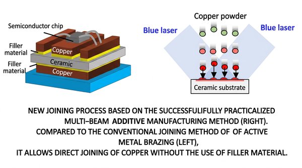
KEY POINTSShimadzu, Osaka University and DOWA Power Device commercialize copper-AlN substrates using a multi-beam additive manufacturing processBlue semiconductor laser method directly coats copper on AlN without silver, aiming to reduce insulation failures and residual stressHeat-cycle durability improves more than threefold versus conventional substrates, with target uses in power semiconductors, AI servers and optical communications
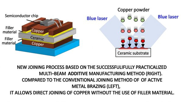
A diagram shows the new multi-beam additive manufacturing process for copper-AlN substrates. Note: Japanese text in the original image from press release has been translated into English by our editorial team.
Shimadzu Corp.
Shimadzu Corp. said on Aug. 25 it had commercialized a copper-aluminum nitride substrate produced with a multi-beam additive manufacturing method developed jointly with Osaka University’s Joining and Welding Research Institute and DOWA Power Device Co., a group company of DOWA Holdings.
The process directly coats copper electrodes onto an aluminum nitride, or AlN, substrate by simultaneously irradiating copper powder and a blue semiconductor laser, eliminating the use of silver that can cause insulation failures. Shimadzu described it as the world’s first such technology.
Copper-AlN substrates are used mainly as heat-dissipating insulators in power semiconductor devices because they combine thermal conductivity with electrical insulation. Conventional joining methods typically use high-temperature bonding with silver-containing brazing material, which has posed challenges including long production times, residual stress and the risk of silver migration that can undermine insulation reliability.
The three parties have conducted joint research since November 2022. Shimadzu has been responsible for developing the copper-coating equipment using blue semiconductor lasers and the manufacturing process.
The multi-beam additive manufacturing method can join ceramic materials and copper circuits of arbitrary shapes without silver while maintaining strong bonding and low residual stress, the company said. Blue semiconductor lasers have high light absorption efficiency for metals and are suited to processing pure copper.
The resulting substrates deliver high heat dissipation performance and more than triple the heat-cycle durability of conventional substrates, according to the release. The use of 3D manufacturing technology also enables fine-line patterns and complex circuit shapes.
Power semiconductors are used in applications including electric vehicles, industrial equipment and power conversion systems, where thermal management is a critical design factor. AlN has long been used in electronic substrates because it offers relatively high thermal conductivity among ceramics while retaining electrical insulation.
Shimadzu said it will continue verification work for applications requiring dense wiring and miniaturization, including optical communications equipment, communications satellites, AI servers and medical lasers.
AloJapan.com