

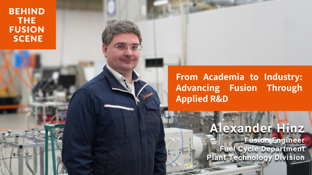
In a nutshell:
Since joining KF in September 2024, Alexander has been contributing to the development of sensors capable of detecting hydrogen isotopes by drawing on his broad experiences working on vacuum technology, low temperature plasma, and semiconductors—knowledge he has built through a decade of academic research in Germany and the UK.
Could you tell us about your role at Kyoto Fusioneering (KF)?
As a Fusion Engineer in the Tritium Technology Team within the Fuel Cycle Department, I focus primarily on developing tritium extraction systems and tritium sensors. I’m currently working on two main projects.
The first is the development of the Hydrogen Isotope Permeation Sensor (HPS) for monitoring tritium in breeding blankets, a project led by our colleagues in the UK. While the core concept has already been validated internally, we are now tackling challenges within our UNITY‑1’s liquid metal loop. In particular, the sensor installed near the inlet of the Vacuum Sieve Tray (VST) —which extracts the hydrogen isotopes generated in the breeding blanket—must remain fully submerged in the liquid metal lithium‑lead alloy. This is a big operational challenge, and we are working to solve it.
The second project involves an electrochemical sensor. The technology originates from a 20‑year‑old design created by a Japanese company to detect hydrogen in metal casting and prevent structural defects caused by hydrogen bubbles. I’m working closely with our business team and Japanese manufacturers to adapt and optimize this sensor for fusion applications.
Because we’re developing technologies that have never existed before, we constantly run simulations, conduct experiments, and iterate on the designs. We rarely get the expected results right away. But when I encounter an unexpected setback, I find it more fascinating than frustrating—this is the essence of R&D, and discovering new data through experiments is incredibly rewarding.
Although I had no prior experience in fusion, I’ve been able to fully leverage my background in materials science and vacuum technology.
You have experience in diverse fields. How did you first become interested in them?
Even though my father was an engineer, I initially had no clear intention of becoming one. In high school, I considered many paths—including joining the German military or going to law school.
My brother ended up influencing me the most. He was studying science at Kiel University in Germany, so I looked up the university and discovered the departments of electrical engineering and materials science. I wasn’t sure what I wanted to pursue, so I chose materials science that would offer a broad mix of physics, chemistry, and engineering courses, which would allow me to find what I want to pursue later.
One of my classes was a vacuum technology course taught by a Russian physicist who had formerly directed an institute in Moscow. His lectures were captivating, and I quickly developed a deep interest in the field.
At the time, I was searching for a student assistant position to expand my practical knowledge, and he offered me a role because I had performed well in his course. That opportunity marked the beginning of my specialization in vacuum engineering, and I became immediately excited about its broad applicability across many industries.
When you started your research career in vacuum technology, what kind of work were you doing in the lab?
My early work involved thin‑film technologies used in the semiconductor industry. I applied various vacuum deposition methods—including magnetron sputtering and thermal evaporation deposition—to produce thin metal and polymer composite films.
Later, during my Ph.D., I worked on fundamental research related to the formation of dust particles in low‑temperature plasma, which contrasts with the high‑temperature plasmas used in fusion.
My lab work sparked a strong interest in semiconductors, given how essential they are to modern life. During my Ph.D., I spent some time at Kyushu University in Japan because my supervisor was a guest professor there. I worked on growing zinc oxide layers on silicon, which can eventually be overgrown with gallium nitride. In simple terms, I created extremely thin, precise layers of materials so they can be combined into advanced electronic components like LEDs, sensors, and high-efficiency power devices.
My initial time in Japan gave me a strong sense of cultural fit, so the idea of building my career here kept resurfacing over the years.
As I was finishing my Ph.D., I tried to enter the semiconductor industry in Europe and in Japan because I wanted to contribute to a technology with real industrial impact.
However, despite applying to several companies, I wasn’t hired. Honestly speaking, I was disappointed, but I realized it simply might not have been the right time. So, I chose to continue as a postdoc to strengthen my semiconductor experience. This led me to a two‑year position at the University of Cambridge, where I researched wide band‑gap semiconductor growth.
After continuing in academia, when and what guided you back toward industry?
Even after Cambridge, I remained in academia because of my earlier struggles entering industry.
Fortunately, my Ph.D. supervisor whom I was keeping in touch with, forwarded me a job announcement from the Fraunhofer Institute in Germany seeking expertise that closely matched my previous work. Therefore, I continued my research there for another four years.
Still, I wasn’t ready to give up on working in industry because the more I advanced in my research, the stronger my desire grew to make a real impact in industry. So, I started searching more broadly—not only in semiconductors but also in areas where I could apply my strengths, such as vacuum technology. That’s when I discovered opportunities in fusion engineering.
Were you already familiar with fusion?
I had heard of it because Kiel University is close to the Max Planck Institute in Greifswald, where the Wendelstein 7‑X stellarator (W7-X) operates. It is also one of the few universities in Germany offering large‑scale plasma physics education.
As a student, I had the chance to visit the Max Planck Institute when W7‑X was still under construction, and I became deeply interested in fusion once I realized how it could genuinely help address some of our most pressing environmental challenges. So even during my time at Cambridge, I continued to follow its progress.
There are several fusion companies and national labs. What made you choose KF?
KF’s unique business model immediately appealed to me, but discovering the company in the first place happened purely by chance.
When I was job‑hunting in semiconductors, I had registered on global job platforms and looked for opportunities in Japan. However, at that time, it was still uncommon for international engineers to work in R&D roles in Japan. Later, while browsing online, I came across KF.
I looked at KF’s website and when I found out that it focuses on fusion plant engineering rather than plasma physics, I felt confident I could contribute with my experiences. So, I immediately applied for an Engineer position because I had strong confidence this time that I could contribute directly to the development of KF’s R&D in topics such as the fusion fuel cycle system, which is essential for sustainable operation of fusion power plant.
After clearly and passionately conveying my motivation in my application and during the interview, I was fortunately given the chance to join the team.
How do you feel now that you’re working at KF in Japan?
Working at KF has confirmed what I had expected—that my background in semiconductors and vacuum technology truly helps me contribute to sensor development. It’s rewarding to see how experiences I gathered across different fields and countries connect so naturally to what I’m doing now.
In addition, KF is a very international company, and thus my past experiences conducting research in Japan and working in the UK have been invaluable. My past experiences have helped me bridge different working styles and collaborate smoothly with colleagues of various nationalities, which is something I genuinely enjoy.
When I first joined, people told me that Japanese wasn’t essential because many colleagues speak English. That turned out to be partly true, but I quickly realized that being able to communicate in Japanese opens far more doors—especially when working with vendors or colleagues who feel more comfortable in Japanese.
So I began studying the language again, and it’s incredibly satisfying when conversations flow naturally. Moments like that make me feel that I genuinely fit into the culture here and remind me why returning to Japan always felt right.
Lastly, what would you like to achieve at KF and in the fusion field?
My immediate goal is to turn our research into tangible products. I’m working hard to develop the HPS and the electrochemical hydrogen sensor into products that our business team can bring to market.
In the long term, I hope to see the first fusion power plants become reality—and to still have at least decades in my career to witness the development of the second generation of fusion power plants.
■Job Opportunities
■Previous Behind the Fusion Scene
AloJapan.com