
Japan-backed Rapidus accelerates its 2nm push, outlining bold plans to catch up with top global foundries. Reports from Nikkei and Yomiuri Shimbun say while its first Hokkaido Chitose fab has yet to start mass production, the company aims to break ground on a second facility as early as FY2027, targeting 1.4nm chip output in 2029.
Chasing the Giants
If all goes according to plan, Rapidus could be approaching the timelines of TSMC, Intel, and Samsung. The Economic Daily News suggests that TSMC has started construction on the first phase of its A14 (1.4nm) fab in Taiwan’s Central Science Park, targeting mass production in H2 2028. Meanwhile, Wccftech reports that Intel’s 14A has already reached performance and yield levels comparable to 18A, nearly a year ahead of schedule.
On the other hand, the Chosun Biz notes that Samsung has pushed back mass production of its 1.4nm process from 2027 to 2029, focusing instead on boosting yields for its 2nm process. Industry sources cited by the report say Samsung’s 2nm yield has now reached 55–60%, with plans to raise it to 70% by year-end.
Advances 1.4nm/1nm Ambitions with Government Support
Rapidus is not only moving full speed on its 2nm ambitions, with plans to start mass production at its Chitose fab in the latter half of FY2027. According to MoneyDJ, citing Nikkei and Yomiuri Shimbun, the company is already designing mass production lines for a second facility, which will produce 1.4nm chips and potentially 1nm products. Rapidus aims to kick off mass production of 1.4nm and 1nm chips around 2029–2030, the report adds.
According to the reports, Rapidus will begin comprehensive R&D on 1.4nm products starting FY2026, and will continue collaborating with IBM to reveal its mass production roadmap beyond 1.4nm, aiming to secure long-term customers.
The Japanese foundry is certainly getting full support from the government. As per Yomiuri Shimbun, Japan’s Ministry of Economy, Trade and Industry (METI) announced on the 21st that it will invest ¥100 billion in Rapidus this fiscal year through an independent administrative institution, with plans to provide an additional ¥1 trillion in 2026–2027.
Nonetheless, Rapidus notes that although there have been recent media reports regarding construction and operation of a 1.4nm-node semiconductor factory from the firm, these articles are speculation and did not originate from the company. Any updates on Rapidus’s roadmap will come directly from the company and if it decides on any development that should be made public, it will announce it promptly.
Potential Customers
Rapidus’s 1.4nm chips are expected to be used in AI data centers, robotics, autonomous vehicles, and smartphones, as MoneyDJ points out.
Notably, while Fujitsu announced in early October that it would co-develop AI chips with NVIDIA to power Japan’s data centers by 2030, Nikkei XTECH suggests the company is considering Rapidus as a potential manufacturing partner for its 1.4nm-class CPUs designed for AI and high-performance computing, with practical deployment targeted for 2029.
On the other hand, after Rapidus reached a major milestone in July, announcing that prototyping for its 2nm gate-all-around (GAA) chips has begun at the IIM-1 foundry, CEO Atsuyoshi Koike, according to Hokkaido Shimbun, identifies U.S. firms IBM and chip-design startup Tenstorrent as the leading prospective customers.
Read more
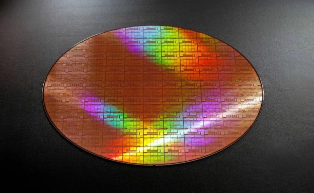
(Photo credit: Rapidus)

Previous Article
[News] Huawei Launches New Mate 80 Series with Kirin 9030, Rumored 7nm 9-Core Chip With 35% Gain
Next Article
[News] SiC Raw Materials See a Price Increase While 6-Inch Substrate Kicks off a Price War
AloJapan.com